Leave Your Message
0%

In the fast-changing world of electronics, semiconductor packaging solutions have really become crucial these days. They now make up around 30% of the total costs in semiconductor manufacturing, and they play a huge role in how well devices perform and how reliable they are. If you’ve seen the latest market reports from SEMI, you’ll notice that the global semiconductor packaging market is expected to hit about $50 billion by 2025. That growth is mainly driven by exciting advancements in 5G, IoT, and AI technology. Take Zhejiang Dron Technology Co., Ltd., for example — founded back in 2004 and recognized as a national high-tech enterprise, we’re right in the middle of this wave of change.
Revolutionizing Electronics: The Essential Guide to Semiconductor Packaging Solutions

We do everything from development and design to research, production, and sales, creating state-of-the-art equipment tailored for all kinds of applications. By offering top-notch semiconductor packaging solutions, we’re not just helping devices perform better — we’re also playing our part in the industry’s growth and pushing toward a more sustainable future.

Understanding Semiconductor Packaging and Its Importance

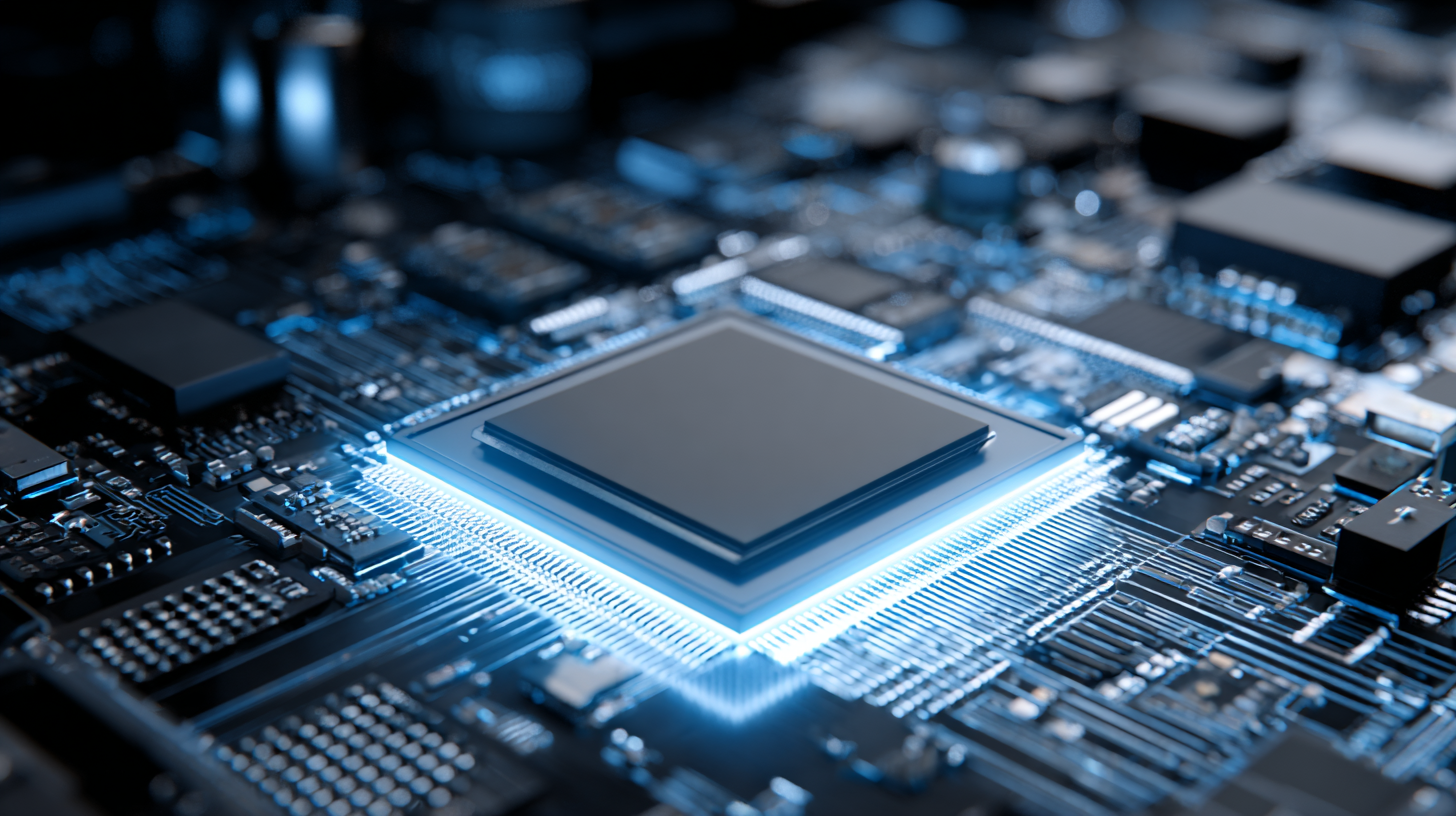
Semiconductor packaging might not be the first thing that comes to mind, but honestly, it's a pretty big deal in today’s electronics world. Think of it like the connector that links the tiny semiconductor chip to everything outside—without it, the chip’s kinda stranded. As demand for cutting-edge semiconductors keeps climbing, the need for smarter, more efficient packaging solutions is becoming clearer than ever.

Lately, we’re seeing big players in the industry putting a real focus on advanced packaging tech to stay ahead of the curve. For example, companies like Intel are pushing forward with chiplet systems—think EMIB and Foveros—embracing modular designs that boost both functionality and efficiency. It’s pretty exciting to see how these innovations are changing the game.

On the global scale, investment in semiconductor packaging is booming. Firms are ramping up their capabilities—SK Hynix, for instance, is expanding its back-end manufacturing facilities, and there’s even a brand-new factory dedicated to advanced packaging. Experts believe the market for these smarter packaging solutions is set to grow big time, mainly because artificial intelligence and other demanding tech are really pushing the envelope for more scalable, reliable chips.

Reports are even saying that advanced packaging isn’t just a nice-to-have anymore; it’s a must-have for staying competitive. Technologies like CoWoS and CPO are leading the way, completely transforming how chips are designed and manufactured. All in all, this evolving packaging scene isn’t just about better performance—it’s also about supporting the complex supply chains that keep the entire global semiconductor industry ticking. Pretty fascinating, huh?

Key Types of Semiconductor Packaging Solutions and Their Applications

Semiconductor packaging is a pretty crucial part of how electronics work — it really impacts performance, reliability, and even the size of the device. When talking about the main types out there, you've got the Dual In-line Package (DIP), Surface Mount Technology (SMT), and Ball Grid Array (BGA). DIP’s been around for ages and is mostly used for through-hole mounting, so you'll see it more in older gadgets. SMT, on the other hand, is a more modern approach — it allows for smaller components and makes manufacturing way more efficient, which totally makes it perfect for compact gadgets these days. Then there's BGA, which steps things up with better thermal and electrical performance — ideal for high-speed, demanding applications.

**Pro tip:** When you're picking a packaging style, consider things like heat management, space limitations, and whether you might need to upgrade down the line.

Another cool option is Chip-on-Board (CoB). It involves attaching bare chips directly to a substrate, which saves space — super handy for tiny stuff like medical devices or smartphones. Plus, if you want to pack multiple functions into one package, System in Package (SiP) is the way to go. It helps cut down on space and makes your electronic assembly less complicated.

**Another tip:** Make sure to think about the environment your chips will be in — choose materials and designs that can handle conditions like temperature, humidity, or vibrations to keep everything running smoothly and avoid unexpected problems.

Revolutionizing Electronics: The Essential Guide to Semiconductor Packaging Solutions

Innovative Materials in Semiconductor Packaging Technology

Hey, have you noticed how the semiconductor world is really going through a big change right now? A lot of that has to do with new materials being used in packaging technology—stuff like advanced polymers, ceramics, and composites. These upgrades are super important because they help devices perform better, last longer, and work more efficiently. Instead of sticking with old methods, manufacturers are now bringing in these new materials to tackle the usual problems. For example, they boost thermal management, cut down electromagnetic interference, and make the whole package more robust—things that are absolutely essential as electronics keep getting more complex and demanding.

Take Zhejiang Dron Technology Co., Ltd., for instance. They've been around since 2004 and really stand out in this space. They're a high-tech company dedicated to pushing the envelope with innovative semiconductor packaging solutions. Their focus on research and clever engineering means they’re always finding ways to improve how semiconductors are designed and made. Using state-of-the-art equipment and these new materials, Dron not only boosts product performance but also helps support a wide range of applications across the electronics world. It’s pretty exciting to see how they’re shaping the future of chip packaging!

Revolutionizing Electronics: The Essential Guide to Semiconductor Packaging Solutions

Challenges in Semiconductor Packaging and Future Solutions

The semiconductor industry is really going through a big change right now, mainly because of the challenges brought on by Moore's Law and the increasing complexity of systems. There's this constant buzz about AI systems getting more advanced, and honestly, that’s pushing innovation in how chips are packaged — it’s become a pretty crucial area. As chips get both more powerful and smaller, we need new packaging solutions to keep things running smoothly and maintain top performance. No wonder the global market for semiconductor packaging is expected to grow a lot — it’s a clear response to all these shifting needs.

So, if you're looking to tackle packaging issues, here are a few tips. First off, think about investing in better thermal management solutions. When chips are stacked in 2.5D or 3D configurations, overheating can really become a headache. Using innovative cooling techniques is a must to keep things reliable. Second, don’t be shy about collaborating more across the supply chain. Working together allows companies to smooth out processes, share best practices, and ultimately get products to market faster and more efficiently. And finally, keep an eye on what's happening with multichip packaging. It’s got some serious potential to boost performance while also bringing costs down, so it’s definitely something to watch for the future.

Overall, it’s an exciting time in the industry, but staying on top of these trends and solutions is key if you want to keep up!

Revolutionizing Electronics: The Essential Guide to Semiconductor Packaging Solutions - Challenges in Semiconductor Packaging and Future Solutions

Challenge Description Current Solutions Future Directions
Miniaturization The need to reduce size while increasing functionality. 3D packaging technologies and system-in-package (SiP) approaches. Integration of more components in a single package and advanced materials.
Thermal Management Dissipation of heat from densely packed semiconductor devices. Use of thermal interface materials and heat sinks. Exploration of advanced cooling methods like micro-channel heat exchangers.
Cost Reduction Maintaining quality while lowering production costs. Lean manufacturing and automation in production processes. Development of cost-effective materials and recycling methods.
Reliability Ensuring products function correctly over time under varying conditions. Rigorous testing protocols and quality assurance measures. Improvement in modeling and simulation for better prediction of failures.
Sustainability The environmental impact of semiconductor manufacturing processes. Adoption of eco-friendly materials and production techniques. Development of biodegradable packaging solutions and lifecycle assessments.

Sustainability Trends in Semiconductor Packaging Practices

The semiconductor world is really gearing up for some big changes, especially as sustainability keeps climbing higher on everyone's radar. You know how folks are loving eco-friendly gadgets these days? Well, manufacturers are catching on and tweaking their practices to be a bit kinder to the planet. We're seeing some pretty cool innovations in materials — like biodegradable options and recyclable stuff — that are becoming more popular. Not only does this make packaging more eco-friendly, but it also lines up with global efforts to cut down waste and support a circular economy. It’s kinda exciting to watch how these small shifts can add up!

According to market predictions, the rise of sustainable electronics and greener manufacturing isn’t slowing down. In fact, the industry is expected to grow quite rapidly — with a projected annual increase of about 15.7% in recycling and sustainability-focused sectors. That’s definitely a sign that more companies are realizing how important effective recycling and sustainable practices are. As they pour more resources into greener tech and smarter processes, there's a growing focus on creating packaging solutions that hit the sweet spot — meeting top-notch performance standards but also staying environmentally responsible. All in all, it’s looking like a brighter, greener future for electronics.

Emerging Technologies Shaping the Future of Electronics Packaging

The semiconductor packaging industry is going through some pretty exciting changes lately. New tech is really pushing things forward, making designs more efficient and way more compact than before. I saw a recent report from MarketsandMarkets that predicts the electronic packaging market will jump from around $31 billion in 2023 to over $39 billion by 2028. That’s mainly because of advances in miniaturization and the booming demand for high-performance gadgets. Techniques like 3D packaging and system-in-package (or SiP for short) are totally changing how we put components together — saving tons of space and boosting overall performance.

As these innovations keep evolving, it’s clear that manufacturers need to keep up if they want to stay competitive. One thing I’d suggest for businesses is to really focus on investing in R&D — exploring new materials and packaging ideas can make a big difference. Using advanced materials like organic substrates or thermally conductive fillers can cut down weight, but also help with heat management, so devices keep running smoothly even under tough conditions. Plus, teaming up with tech partners can spark innovation and help companies stay ahead of the curve.

And let’s not forget about sustainability — it’s becoming a big deal these days. Switching to eco-friendly packaging options isn't just about following regulations; it’s also a smart move because consumers are more conscious of environmental issues. Companies like Intel get it, too. They've committed to cutting packaging waste and boosting recyclability by 2030. So, planning ahead with green solutions isn’t just good for the planet — it’s good for business too.

FAQS

: What are the key types of semiconductor packaging solutions?

: The key types of semiconductor packaging solutions include Dual In-line Package (DIP), Surface Mount Technology (SMT), Ball Grid Array (BGA), Chip-on-Board (CoB), and System in Package (SiP).

What is the primary use of Dual In-line Packages (DIP)?

DIP is mainly used for through-hole mounting and is common in older electronic products.

Why is Surface Mount Technology (SMT) preferred for modern devices?

SMT allows for smaller components and greater efficiency in manufacturing, making it ideal for compact electronic devices.

What advantages does Ball Grid Array (BGA) offer?

BGA provides improved thermal and electrical performance, making it suitable for high-speed applications.

What is the benefit of using Chip-on-Board (CoB) packaging?

CoB attaches bare chips directly to a substrate, offering advantages in space-saving, particularly in applications requiring miniaturization, such as medical devices and mobile technology.

How does System in Package (SiP) enhance electronic assemblies?

SiP integrates multiple functions into a single package, reducing the footprint and complexity of electronic assemblies.

What are some challenges faced in semiconductor packaging today?

Challenges include adhering to Moore's Law, managing increasing system complexity, and meeting the demands of advanced artificial intelligence systems.

What should companies consider to address thermal management concerns in packaging?

Companies should consider investing in advanced thermal management solutions, especially for stacked chip configurations (2.5D and 3D) to prevent overheating.

Why is collaboration across the supply chain important in semiconductor packaging?

Collaboration can streamline processes and share insights, leading to more efficient manufacturing and reduced time to market.

What emerging trend should companies pay attention to in semiconductor packaging?

Companies should keep an eye on multichip packaging trends, which have the potential to enhance chip performance while lowering costs.

Conclusion

In this article, titled "Revolutionizing Electronics: The Essential Guide to Semiconductor Packaging Solutions," we dive into how crucial semiconductor packaging really is in the world of electronics. It’s not just a side note—they play a huge role in making sure our devices work smoothly. We go over the main types of packaging and how each one is used in different electronic gadgets. Plus, we talk about some pretty cool new materials that are pushing packaging tech forward. Of course, it wouldn’t be complete without touching on the current hurdles the industry faces and what potential solutions are on the horizon. Oh, and there's also a look at sustainability trends and emerging tech that are shaping the future of electronics packaging—exciting stuff!

Now, on the business side, Zhejiang Dron Technology Co., Ltd. has been around since 2004. They’re a high-tech company with a real passion for creating top-notch equipment for semiconductor packaging. They do it all—development, design, research, manufacturing, and sales—so they’re in a great position to support the ongoing innovations in this super important area and help drive the industry forward.

Sebastian

Sebastian

Sebastian is a dedicated marketing professional at Zhejiang Delong Technology Co., Ltd., where he brings a wealth of expertise and passion for the company's innovative products. With a strong background in technology and marketing, he excels in creating informative and engaging content that......
Previous Navigating Global Import Compliance for Dron Technology Solutions